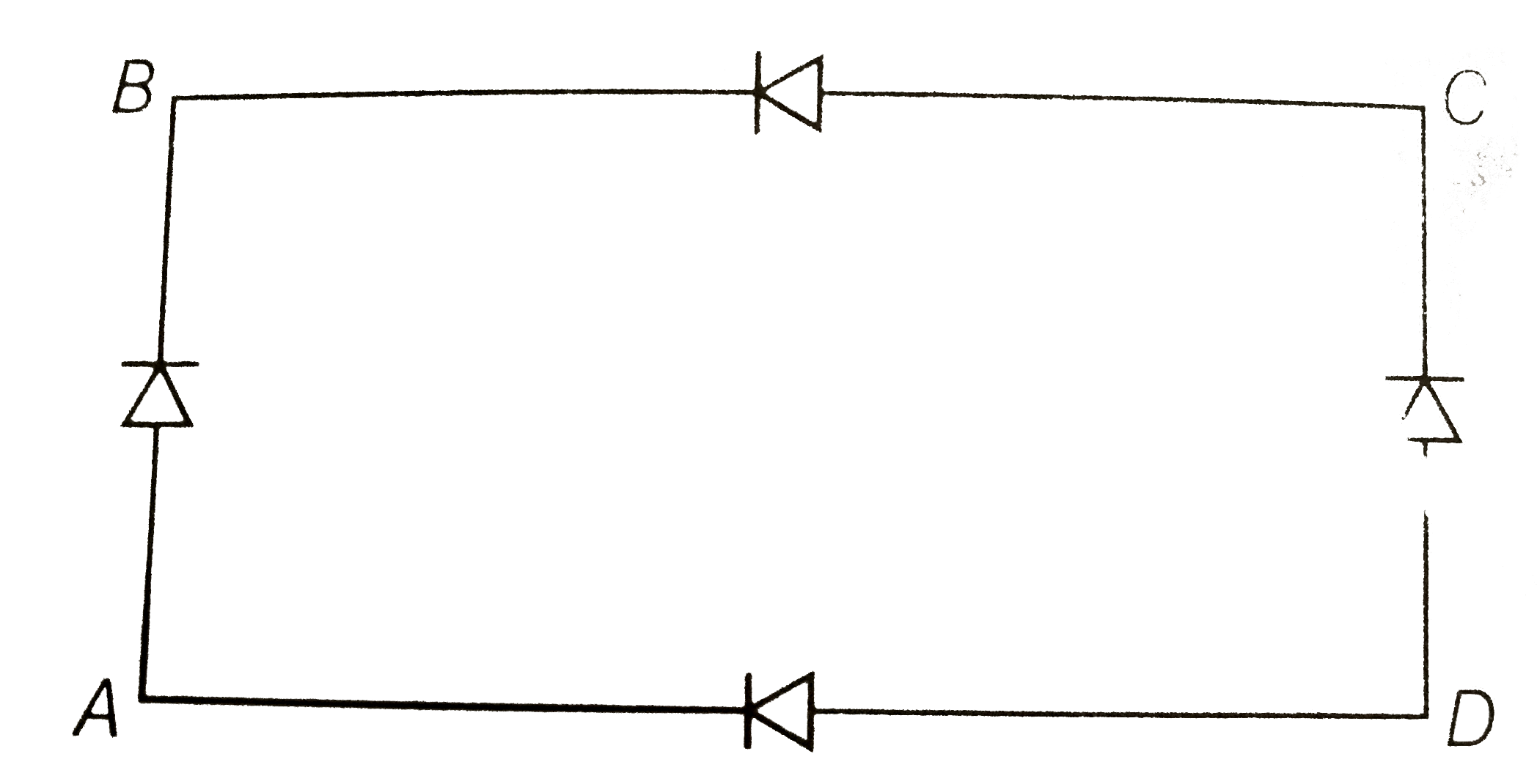
A
B
C
D
Text Solution
Verified by Experts
The correct Answer is:


Topper's Solved these Questions
SEMICONDUCTOR ELECTRONICS (MATERIAL, DEVICES AND SIMPLE CIRUITS )
AAKASH INSTITUTE ENGLISH|Exercise Assignment section -B (Objective Type Question)|29 VideosSEMICONDUCTOR ELECTRONICS (MATERIAL, DEVICES AND SIMPLE CIRUITS )
AAKASH INSTITUTE ENGLISH|Exercise Assignment section -C (Previous years type question)|110 VideosSEMICONDUCTOR ELECTRONICS (MATERIAL, DEVICES AND SIMPLE CIRUITS )
AAKASH INSTITUTE ENGLISH|Exercise EXERCISE|20 VideosRAY OPTICS AND OPTICAL INSTRUMENTS
AAKASH INSTITUTE ENGLISH|Exercise ASSIGNMENT (SECTION - D)|16 VideosSEMICONDUCTOR ELECTRONICS: MATERIALS, DEVICES AND SIMPLE CIRCUITS
AAKASH INSTITUTE ENGLISH|Exercise Assignment (Section-D (Assertion and reason))|5 Videos
Similar Questions
Explore conceptually related problems
AAKASH INSTITUTE ENGLISH-SEMICONDUCTOR ELECTRONICS (MATERIAL, DEVICES AND SIMPLE CIRUITS )-Assignment section -A (Objective Type Question)
- Two identical P-N junctions, may be connected in series with a battery...
Text Solution
|
- Zener diode is used for:-
Text Solution
|
- In figure the input is across the terminals A and C and the output is ...
Text Solution
|
- A junction diode , in which one of the p or n - sections is made very ...
Text Solution
|
- The materials suitable for making a solar cell is
Text Solution
|
- In which of the configuration of a transistor , the power gain is high...
Text Solution
|
- In a common base amplifier the phase difference the input signal volta...
Text Solution
|
- The current transfer ratio beta of a transistor is 100. The input resi...
Text Solution
|
- In a common emitter transistor circuit, the base current is 40 muA , t...
Text Solution
|
- The emitter region in a PNP-junction transistor is more heavily doped ...
Text Solution
|
- A transsitor is operated in CE configuration at V(CC) = 2 V such that ...
Text Solution
|
- The input resistance of a silicon transistor is 665Omega. Its base cur...
Text Solution
|
- The relationship between alpha and beta is given by
Text Solution
|
- In a common base transistor circuit, the current gain is 0.98. On cha...
Text Solution
|
- For a transistor amplifier power gain and voltage gain are 7.5 and 2.5...
Text Solution
|
- The input resistance of a common-emitter amplifier is 2 kOmega and a.c...
Text Solution
|
- In a silicon transistor, a change of 7.89 mA in the emitter current pr...
Text Solution
|
- The abjoining logic symbol is equivalent to
Text Solution
|
- Which of the following gates corresponds to the truth table given belo...
Text Solution
|
- Figure shows two capacitors of capacitance 2muF and 4muF and a cell of...
Text Solution
|