A
B
C
D
Text Solution
Verified by Experts
The correct Answer is:


Topper's Solved these Questions
SEMICONDUCTOR ELECTRONICS (MATERIAL, DEVICES AND SIMPLE CIRUITS )
AAKASH INSTITUTE ENGLISH|Exercise Assignment SECTION - D (Assertion & reason type Question)|10 VideosSEMICONDUCTOR ELECTRONICS (MATERIAL, DEVICES AND SIMPLE CIRUITS )
AAKASH INSTITUTE ENGLISH|Exercise Assignment section -B (Objective Type Question)|29 VideosRAY OPTICS AND OPTICAL INSTRUMENTS
AAKASH INSTITUTE ENGLISH|Exercise ASSIGNMENT (SECTION - D)|16 VideosSEMICONDUCTOR ELECTRONICS: MATERIALS, DEVICES AND SIMPLE CIRCUITS
AAKASH INSTITUTE ENGLISH|Exercise Assignment (Section-D (Assertion and reason))|5 Videos
Similar Questions
Explore conceptually related problems
AAKASH INSTITUTE ENGLISH-SEMICONDUCTOR ELECTRONICS (MATERIAL, DEVICES AND SIMPLE CIRUITS )-Assignment section -C (Previous years type question)
- In the given figure, a dipole D is connected to an external resistance...
Text Solution
|
- The input signal given to a CE amplifier having a voltage gain of 150 ...
Text Solution
|
- Which logic gate is represented by the following combination of logic ...
Text Solution
|
- If in a p-n junction, a square input signal of 10 V is applied as show...
Text Solution
|
- Given then which of the following true
Text Solution
|
- The barrier potential of a p-n junction depends on (i) type of semic...
Text Solution
|
- In a n-type semiconductor, which of the following statement is true ?
Text Solution
|
- In a common emitter (CE) amplifier having a voltage gain G, the transi...
Text Solution
|
- The output (X) of the logic circuit shown in figure will be
Text Solution
|
- Two ideal diodes are connected to a battery as shown in the circuit. T...
Text Solution
|
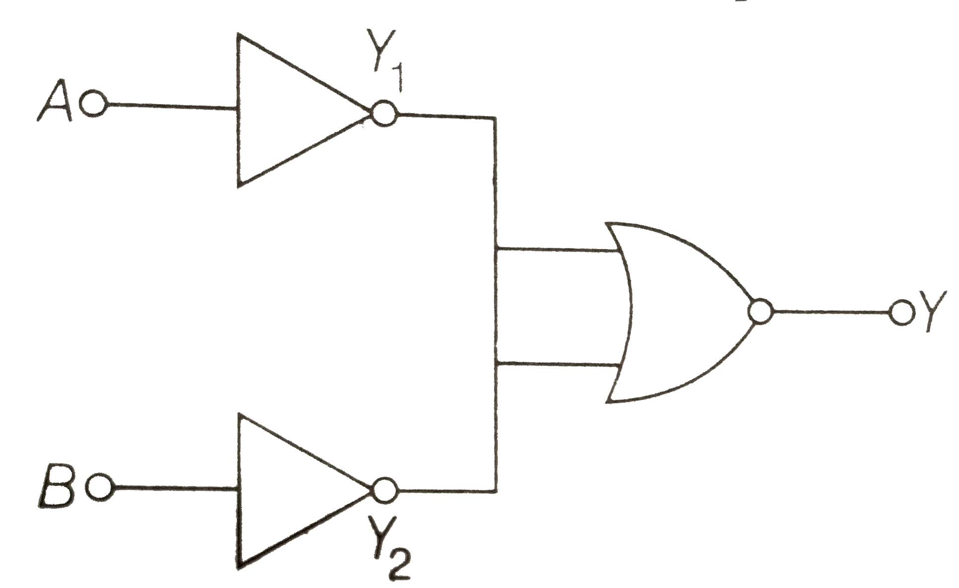
- The figure shows a logic circuit with two inputs A and B and the outpu...
Text Solution
|
- In a CE transistor amplifier, the audio signal voltage across the coll...
Text Solution
|
- C and Si both have same lattice structure, having 4 bonding electrons ...
Text Solution
|
- Transfer characteristic [output voltage (V(0)) vs input voltage (V(i))...
Text Solution
|
- The input resistance of a silicon transistor is 100 Omega. Base curre...
Text Solution
|
- To get an output Y=1 in given circuit which of the following input wil...
Text Solution
|
- A transistor is operated in common emitter configuration at V(c)=2 V s...
Text Solution
|
- If a small amount of antimony is added to germanium crystal
Text Solution
|
- In forward biasing of the p-n junction
Text Solution
|
- Symbolic representation of four logic gates are shown as (i) Pic...
Text Solution
|