A
B
C
D
Text Solution
Verified by Experts
The correct Answer is:


Topper's Solved these Questions
SEMICONDUCTOR ELECTRONICS (MATERIAL, DEVICES AND SIMPLE CIRUITS )
AAKASH INSTITUTE ENGLISH|Exercise Assignment SECTION - D (Assertion & reason type Question)|10 VideosSEMICONDUCTOR ELECTRONICS (MATERIAL, DEVICES AND SIMPLE CIRUITS )
AAKASH INSTITUTE ENGLISH|Exercise Assignment section -B (Objective Type Question)|29 VideosRAY OPTICS AND OPTICAL INSTRUMENTS
AAKASH INSTITUTE ENGLISH|Exercise ASSIGNMENT (SECTION - D)|16 VideosSEMICONDUCTOR ELECTRONICS: MATERIALS, DEVICES AND SIMPLE CIRCUITS
AAKASH INSTITUTE ENGLISH|Exercise Assignment (Section-D (Assertion and reason))|5 Videos
Similar Questions
Explore conceptually related problems
AAKASH INSTITUTE ENGLISH-SEMICONDUCTOR ELECTRONICS (MATERIAL, DEVICES AND SIMPLE CIRUITS )-Assignment section -C (Previous years type question)
- The following figure shows a logic gate circuit with two inputs A and ...
Text Solution
|
- The vapour pressure of two pure liquids A and B that forms an ideal so...
Text Solution
|
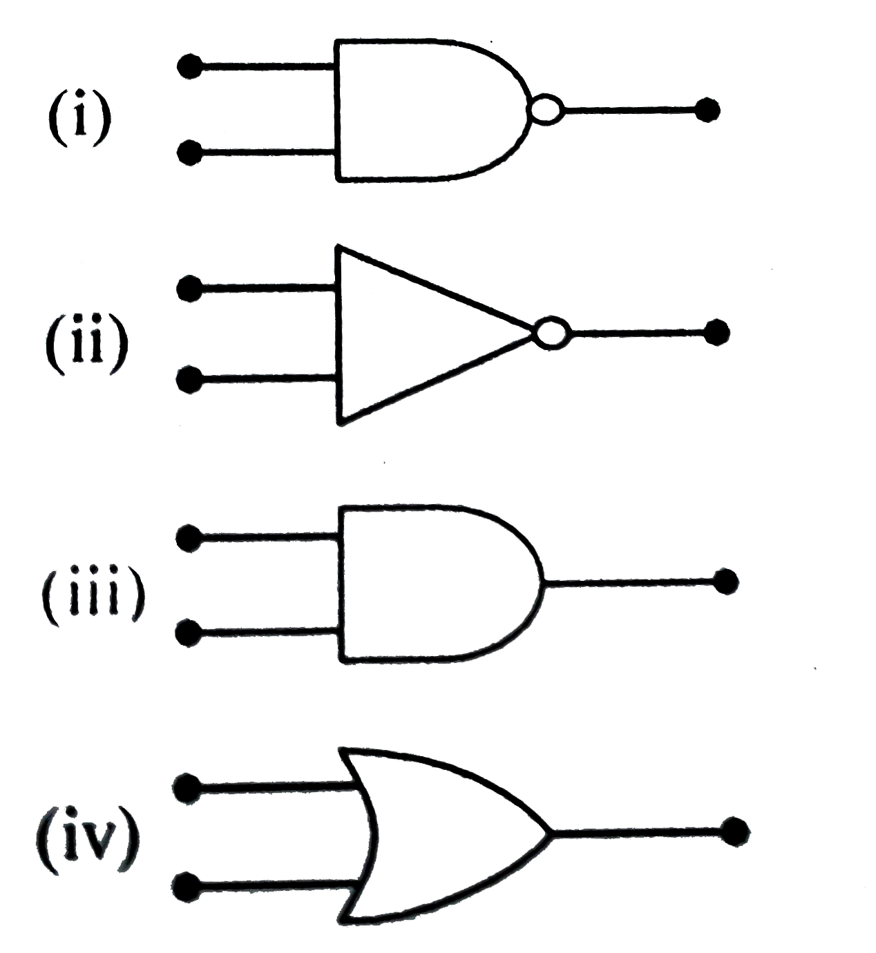
- The symbolic representation of four logic gates are given below : ...
Text Solution
|
- A p-n Photodiode is fabricated from a semiconductor with a band gap of...
Text Solution
|
- A transistor is operated in common-emitter configuration at V(c) = 2 v...
Text Solution
|
- Sodium has body centred packing. Distance between two nearest atoms is...
Text Solution
|
- If the lattice parameter for a crystalline structure is 3.6Å, then the...
Text Solution
|
- The voltage gain of an amplifier with 9% negative feedback is 10. The ...
Text Solution
|
- The circuit
Text Solution
|
- A p-n photodiode is made of a material with a band gap of 2.0 eV. The ...
Text Solution
|
- In the energy band diagram of a material shown below, the open circles...
Text Solution
|
- A common emitter amplifier has a voltage gain of 50, an input impedanc...
Text Solution
|
- In the following circuit, the output Y for all possible inputs A and B...
Text Solution
|
- For a cubic crystal structure which one of the following relation indi...
Text Solution
|
- A transistor is operated in common emitter configuration at constant c...
Text Solution
|
- A forward biased diode is
Text Solution
|
- The following figure shows a logic gate circuit with two inputs A and ...
Text Solution
|
- Application of forward bias to p-n junction
Text Solution
|
- Zener diode is used for:-
Text Solution
|
- Carbon, silicon and germanium have four valence electrons each. These ...
Text Solution
|