Home
Class 12
PHYSICS
In the energy band diagram of a material...

In the energy band diagram of a material shown below, the open circles and filled circles denote holes and electrons respectively. The material is:-

A

An n-type semiconductor

B

A p-type semiconductor

C

An insulator

D

A metal

Text Solution

Verified by Experts

The correct Answer is:
B
Promotional Banner

Topper's Solved these Questions

  • SEMICONDUCTOR ELECTRONICS (MATERIAL, DEVICES AND SIMPLE CIRUITS )

    AAKASH INSTITUTE ENGLISH|Exercise Assignment SECTION - D (Assertion & reason type Question)|10 Videos
  • SEMICONDUCTOR ELECTRONICS (MATERIAL, DEVICES AND SIMPLE CIRUITS )

    AAKASH INSTITUTE ENGLISH|Exercise Assignment section -B (Objective Type Question)|29 Videos
  • RAY OPTICS AND OPTICAL INSTRUMENTS

    AAKASH INSTITUTE ENGLISH|Exercise ASSIGNMENT (SECTION - D)|16 Videos
  • SEMICONDUCTOR ELECTRONICS: MATERIALS, DEVICES AND SIMPLE CIRCUITS

    AAKASH INSTITUTE ENGLISH|Exercise Assignment (Section-D (Assertion and reason))|5 Videos

Similar Questions

Explore conceptually related problems

Which of the energy band diagrams shown in the figure corresponds to that of a semiconductor?

Assertion: If there is some gap between the conduction band and the valence band, electrons in the valence band all remain bound and no free electrons are available in the conduction band. Then the material is an insulator. Reason: Resistance of insulators is very low

A parallel plate capacitor of plate area A and separation d is filled with two materials each of thickness d/2 and dielectric constants in_1 and in_2 respectively. The equivalent capacitance will be

If p is the resistivity of a material, and n is the number density of free electrons in it, the mean time between collisions between electrons in the material is given by: (m denotes the mass of an electron, and e denotes the charge on an electron)

The system shown in the figure diagrams labelled (1), (2) and (3) below represent respectively

In a semiconducting material the mobilities of electrons and holes are mu_(e) and mu_(h) respectively. Which of the following is true?

Draw the Energy bands 'diagrams for a (i) pure semiconductor , (ii) insulator , How does the energy band, for a pure semiconductor , get affected when this semiconductor is doped with (a) an acceptor impurity (b) donor impurity ? Hence discuss why the 'holes' and the 'electrons' respectively, become the 'majority change carries' in these two cases ? Write the two processes involved in the formation of p-n junction.

The hysteresis curve for a material is shown in the figure. Then for the material retentivity, coercivity and saturation magnetization respectively will be

The hysteresis curve for a material is shown in the figure. Then for the material retentivity, coercivity and saturation magnetization respectively will be

Two vessels of different materials are similar in size in every respect. The same quantity of ice filled in them gets melted in 20 minutes and 40 minutes respectively. The ratio of thermal conductivities of the metals is

AAKASH INSTITUTE ENGLISH-SEMICONDUCTOR ELECTRONICS (MATERIAL, DEVICES AND SIMPLE CIRUITS )-Assignment section -C (Previous years type question)
  1. The circuit

    Text Solution

    |

  2. A p-n photodiode is made of a material with a band gap of 2.0 eV. The ...

    Text Solution

    |

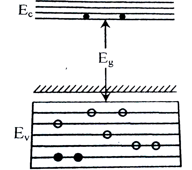
  3. In the energy band diagram of a material shown below, the open circles...

    Text Solution

    |

  4. A common emitter amplifier has a voltage gain of 50, an input impedanc...

    Text Solution

    |

  5. In the following circuit, the output Y for all possible inputs A and B...

    Text Solution

    |

  6. For a cubic crystal structure which one of the following relation indi...

    Text Solution

    |

  7. A transistor is operated in common emitter configuration at constant c...

    Text Solution

    |

  8. A forward biased diode is

    Text Solution

    |

  9. The following figure shows a logic gate circuit with two inputs A and ...

    Text Solution

    |

  10. Application of forward bias to p-n junction

    Text Solution

    |

  11. Zener diode is used for:-

    Text Solution

    |

  12. Carbon, silicon and germanium have four valence electrons each. These ...

    Text Solution

    |

  13. Choose the false statement from the following.

    Text Solution

    |

  14. Copper has face-centered cubic (fcc) lattice with interatomic spacing ...

    Text Solution

    |

  15. The cations and anions are arranged n alternate form in:

    Text Solution

    |

  16. In semiconductors at a room temperature

    Text Solution

    |

  17. In good conductors of electricity the type of bonding that exist is

    Text Solution

    |

  18. In an insulator, the forbidden energy gap between the valence band and...

    Text Solution

    |

  19. In a p-n junction depletion region has a thickness of the order of

    Text Solution

    |

  20. Pure Si at 300 K has equal electron (n(e)) and hole (n(h)) concentrati...

    Text Solution

    |