


AAKASH INSTITUTE ENGLISH-Mock Test 40: PHYSICS-Example
- The symbol of p-n-p transistor is
Text Solution
|
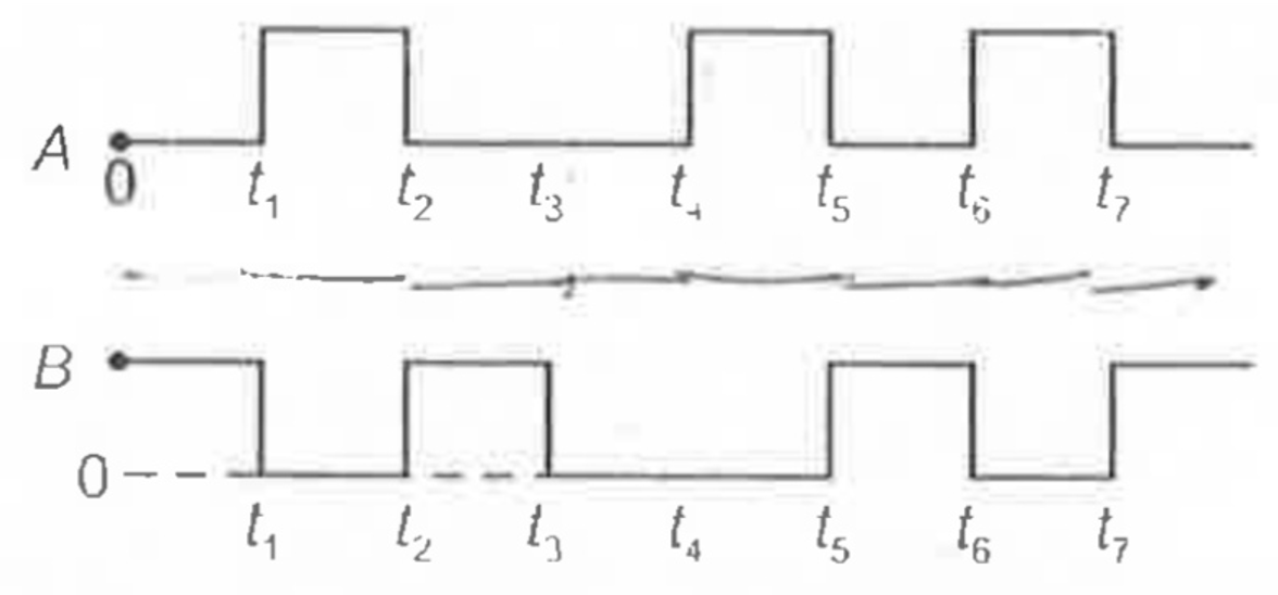
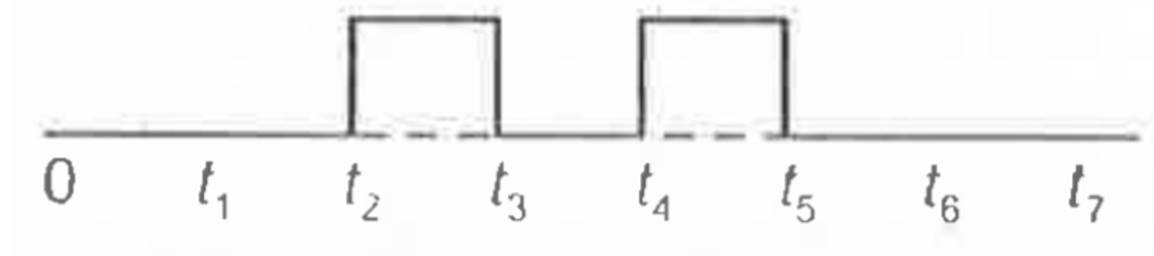
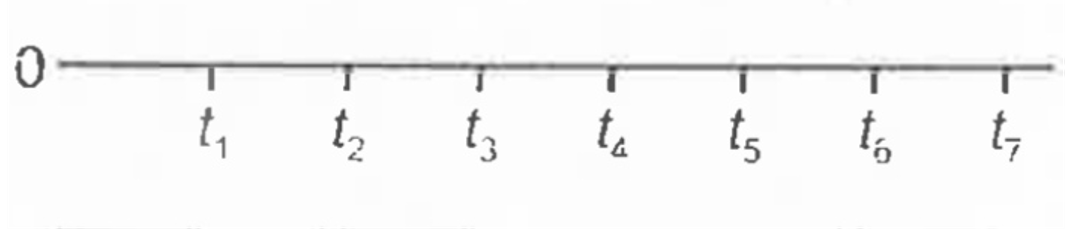
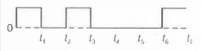
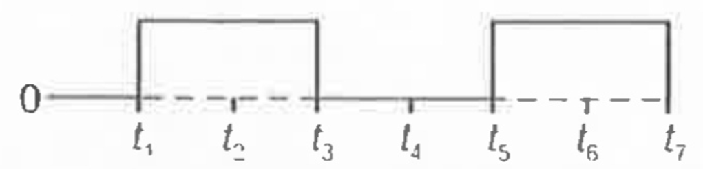
- The output waveform of AND gate for the following input waveforms is
Text Solution
|
- The following truth table corresponds to
Text Solution
|
- The output Y for logic diagram shown below is
Text Solution
|
- The output of the following logic circuit is
Text Solution
|
- The logic circuit (figure) represents which logic gate?
Text Solution
|
- In a common emitter amplifier, the input and output voltage are out of...
Text Solution
|
- A CE amplifier has voltage gain of 50, an input impedance of 2000 ohm ...
Text Solution
|
- The number of terminals in n-p-n transistor is
Text Solution
|
- An AND gate can be prepared by repetitive use of
Text Solution
|
- For a transistor, in a common emitter arragement, the alternating curr...
Text Solution
|
- Transistors can work as a switch in
Text Solution
|
- Transconductance in CE amplifier circuit is defined as
Text Solution
|
- Power Gain of CE amplifier circuit is given by
Text Solution
|
- The following gate is equivalent to
Text Solution
|
- The element X and Y in the communication system (figure) are respectiv...
Text Solution
|
- The length of half wave dipole antenna at 50 MHz is
Text Solution
|
- The process of increasing the strength of a signal using an electronic...
Text Solution
|
- A device that converts one from of energy into another form is termed ...
Text Solution
|
- The power radiated by linear antenna of length 'l' is proportional to ...
Text Solution
|