A
B

C
D
Text Solution
Verified by Experts
The correct Answer is:


Topper's Solved these Questions
Similar Questions
Explore conceptually related problems
RESONANCE ENGLISH-SEMICONDUCTORS-Exercise 3
- A working transistor with its three legs marked P, Q and R is tested u...
Text Solution
|
- In the circuit below, A and B represent two inputs and C represents th...
Text Solution
|
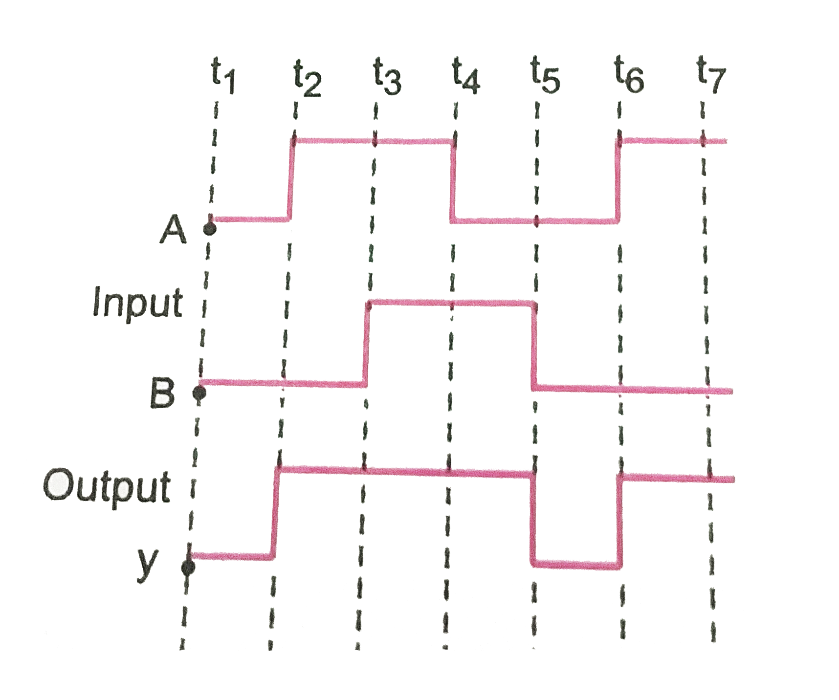
- The Fig shown input waveforms A and B to a logic gate. Draw the output...
Text Solution
|
- A p -n junction (D) shown in the figure can act as a rectifier. An alt...
Text Solution
|
- The output of an OR gate is connected to both the inputs of a NAND gat...
Text Solution
|
- Truth table for system of four NAND gates as shown in figure is
Text Solution
|
- The I - V characteristic of an LED is
Text Solution
|
- The forward biased diode connection among the following is
Text Solution
|
- Two identical P-N junctions, may be connected in series with a battery...
Text Solution
|
- In a p- n junction diode not connected to any circuit,
Text Solution
|
- For the given circult shown in fig to act as full wave rectifer , the ...
Text Solution
|
- In a....... baised pn junction , the net flow of holes is from the n ...
Text Solution
|
- The cause of the potential barrier in a p-n diode is
Text Solution
|
- The transfer ratio of a transistor is 50. The input resistance of the...
Text Solution
|
- When added an impurity into the silicon which one of the following pro...
Text Solution
|
- In a junction diode, the holes are due to
Text Solution
|
- A p-type semiconductor is
Text Solution
|
- The following circuit represents
Text Solution
|
- The current (I) in the circuit will be:-
Text Solution
|
- Copper and silicon is cooled from 300 K to 60 K, the specific resistan...
Text Solution
|