Home
Class 12
PHYSICS
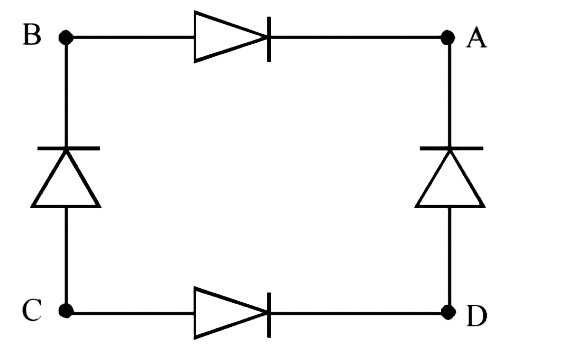
For the given circult shown in fig to ac...

For the given circult shown in fig to act as full wave rectifer , the ac input should be connected across …… and ……. And the d. c output would supplied across …….. And ……….

A

Option1 A,C and B,D

B

Option2 B,D and A,C

C

Option3 A,B and C,D

D

Option4 C,A and D,B

Text Solution

Verified by Experts

The correct Answer is:
B
Promotional Banner

Topper's Solved these Questions

  • SEMICONDUCTORS

    RESONANCE ENGLISH|Exercise Exercise 2|16 Videos
  • REVISION DPP

    RESONANCE ENGLISH|Exercise All Questions|463 Videos
  • SIMPLE HARMONIC MOTION

    RESONANCE ENGLISH|Exercise Advanced Level Problems|13 Videos

Similar Questions

Explore conceptually related problems

When an a.c source is connected across a resistor

Which of the following circuits provides full wave rectification of an ac input?

In the circuit shown there are n repetitions of the same loop. What resistance R _(0) should be connected across the end points , so that the equivalent resistance between a and b may be independent of n ? What is this equal to ?

What is the change in experiment if battery is connected between B and D and galvanometer is connected across A and C ?

A sinusoidal voltage of peak value 200 volts is connected to a diode and resistor R in the circuit shown so that half wave rectification occurs. If the forward resistance of the diode is negligible compared to R the rms voltage (in volt) across R is approximately

A full wave rectifier circuit along with the input and output are shown in Fig. the concentrations from the diode I is (are)

Cells of emfs 10V and 20V are connected as shown. When an ammeter is connected across A and B its reads 1A, when connected across B and C it reads 5, when connected across A and C it reads 3A, find the resistance of the ammeter (in Omega )

Consider the diagram shown below. A Voltmeter of resistance 150 Omega is connected across A and B. The potential drop across B and C measured by voltmeter is

Consider the circuit shown in figure.Find (a) the current in the circuit, (b) the potential drop across the (5 Omega) resistor,(c )the potential drop across the 10(Omega) resistor.(d)Answer the parts (a),(b)and (c )with reference to figure.

For the given combination of gates, if the logic states of inputs A,B,C, are as follows A=B=C=0 and A=B=1, C=0 then the logic states of output D are

RESONANCE ENGLISH-SEMICONDUCTORS-Exercise 3
  1. Two identical P-N junctions, may be connected in series with a battery...

    Text Solution

    |

  2. In a p- n junction diode not connected to any circuit,

    Text Solution

    |

  3. For the given circult shown in fig to act as full wave rectifer , the ...

    Text Solution

    |

  4. In a....... baised pn junction , the net flow of holes is from the n ...

    Text Solution

    |

  5. The cause of the potential barrier in a p-n diode is

    Text Solution

    |

  6. The transfer ratio of a transistor is 50. The input resistance of the...

    Text Solution

    |

  7. When added an impurity into the silicon which one of the following pro...

    Text Solution

    |

  8. In a junction diode, the holes are due to

    Text Solution

    |

  9. A p-type semiconductor is

    Text Solution

    |

  10. The following circuit represents

    Text Solution

    |

  11. The current (I) in the circuit will be:-

    Text Solution

    |

  12. Copper and silicon is cooled from 300 K to 60 K, the specific resistan...

    Text Solution

    |

  13. In a P-N junction diode which is not connected to any circuit-

    Text Solution

    |

  14. For a transistor IC/IE=0.96, then current gain for common emitter conf...

    Text Solution

    |

  15. For the given circuit of p-n-junction diode, which of the following st...

    Text Solution

    |

  16. Barrier potential of a p-n junction diode does not depend on -

    Text Solution

    |

  17. Of the diodes shown in the following figures, which one is reverse bia...

    Text Solution

    |

  18. In semiconductors at a room temperature

    Text Solution

    |

  19. The output of OR gate is 1 :-

    Text Solution

    |

  20. Zener diode is used as

    Text Solution

    |