Home
Class 12
PHYSICS
(a) Draw the circuit diagram of reversed...


(a) Draw the circuit diagram of reversed bias p-n junction.
(b). Draw the output wavefrom across diode in given circuit.
(c). Draw the truth table for the given logic gate.

Text Solution

Verified by Experts

(a).

In reversed biased p-n junction positive terminal of the battery is connected to the n-side of diode and negative terminal of the battery is connected to p-side of diode.
(b). When input voltage is `-5V` the diode is reverse biased and no output is obtained. On the other hand when input is `+5V` the diode is forward biased and output is obtained which is `+5V` therefore,t he output wave from is shown in the figure.
(c) The given circuit is a combination of AND and NOT gate (NAND gate). The truth table will be as shown below:
`{:(A,B,A.B,Y=A.B),(1,1,1,0),(0,1,0,1),(1,0,0,1),(0,0,0,1):}`
Promotional Banner

Topper's Solved these Questions

  • SEMICONDUCTORS

    RESONANCE ENGLISH|Exercise Exercise 2|16 Videos
  • REVISION DPP

    RESONANCE ENGLISH|Exercise All Questions|463 Videos
  • SIMPLE HARMONIC MOTION

    RESONANCE ENGLISH|Exercise Advanced Level Problems|13 Videos

Similar Questions

Explore conceptually related problems

Truth table for the given circuit is

Draw the truth table of a NOR gate.

Truth table for the given circuit (Fig.)is

Truth table for the given circuit (Fig.)is

The output of the given logic circuit is

The truth table for the circuit given in the fig. is

Draw the circuit diagram of a half - wave rectifier using a p-n junction diode.

Output at terminal Y of given logic circuit.

For given logic gate truth table is

Draw a labelled circuit diagram of a half wave rectifier and give its output waveform.

RESONANCE ENGLISH-SEMICONDUCTORS-Exercise 3
  1. A p-n Photodiode is fabricated from a semiconductor with a band gap of...

    Text Solution

    |

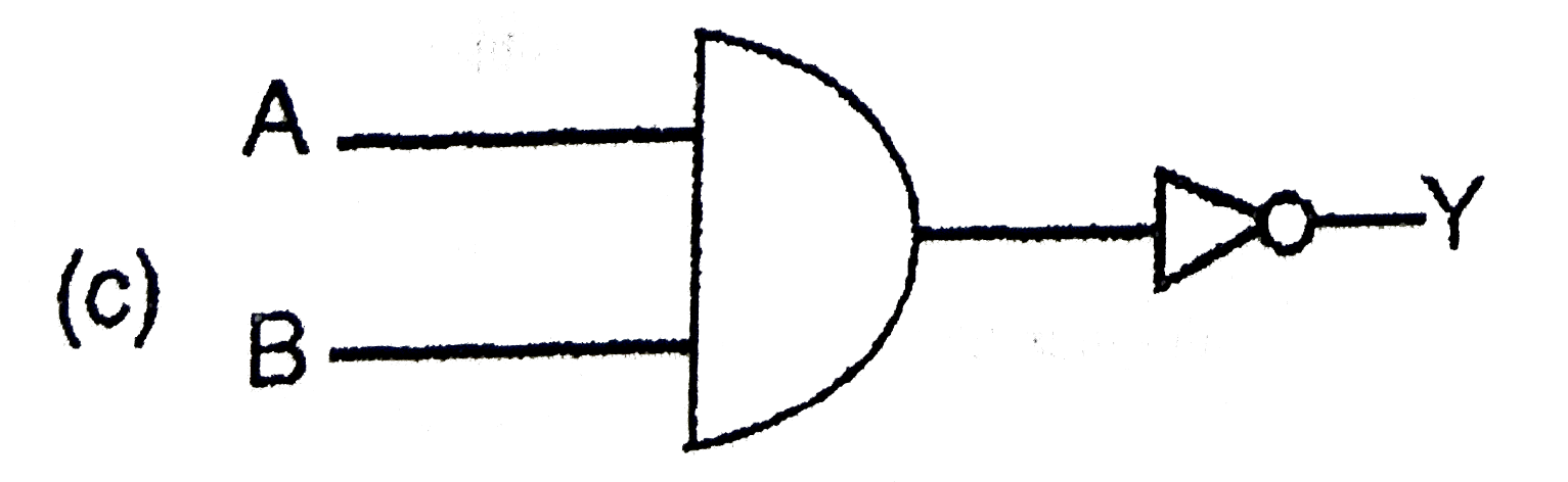
  2. The symbolic representation of four logic gates (i) The logic sym...

    Text Solution

    |

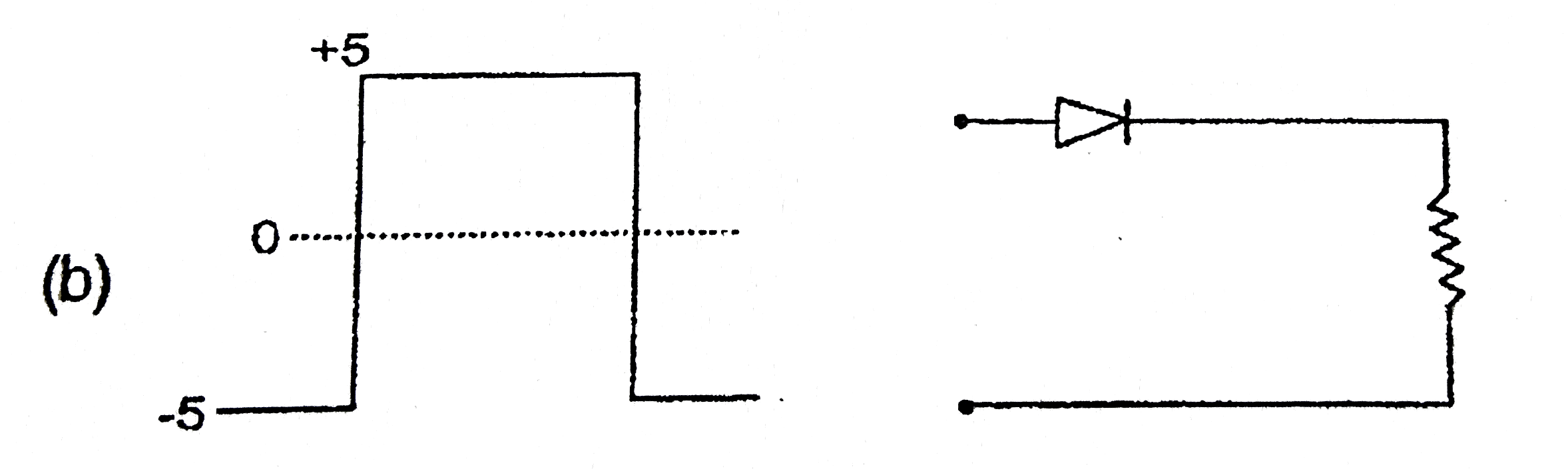
  3. (a) Draw the circuit diagram of reversed bias p-n junction. (b). Dra...

    Text Solution

    |

  4. Which one of the following statement is false?

    Text Solution

    |

  5. The device that can act as a complete electronic circuit is

    Text Solution

    |

  6. A common emitter amplifier has a voltage gain of 50, an input impedanc...

    Text Solution

    |

  7. To get an output 1 from the circuit shown in figure the input must be ...

    Text Solution

    |

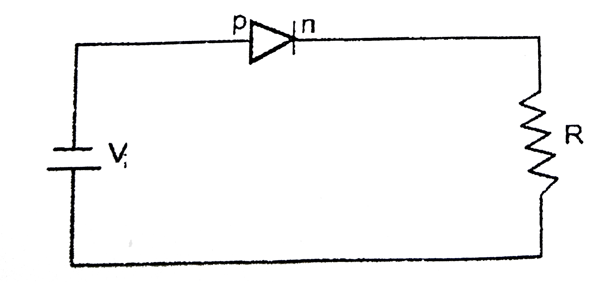
  8. In the following figure, the diodes which are forwards biased are :

    Text Solution

    |

  9. Pure Si at 500 K has equal number of electron (n(e)) and hole (n(h)) c...

    Text Solution

    |

  10. A zener diode having breakdown voltage equal to 15V, is used in a volt...

    Text Solution

    |

  11. A transistor is operated in common-emitter configuration at V(c) = 2 v...

    Text Solution

    |

  12. In forward biasing of the p-n junction

    Text Solution

    |

  13. If a small amount of antimony is added to germanium crystal

    Text Solution

    |

  14. Value of forbidden energy gap for semi conductor is:

    Text Solution

    |

  15. Ga As is a/an:

    Text Solution

    |

  16. The number of free electrons is Si at normal temperature is

    Text Solution

    |

  17. Regarding a semiconductor which one of the following statements is wro...

    Text Solution

    |

  18. For making p-n junction diode forward biased:

    Text Solution

    |

  19. In good conductors of electricity the type of bonding that exist is

    Text Solution

    |

  20. Which of the following statements is true for an n-type semi-comductor...

    Text Solution

    |