A
B
C
D
Text Solution
Verified by Experts
The correct Answer is:


Topper's Solved these Questions
Similar Questions
Explore conceptually related problems
VMC MODULES ENGLISH-JEE MAIN REVISION TEST- 16-PHYSICS (SECTION 2)
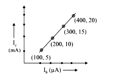
- The transfer characteristic curve of a transistor, having input and ou...
Text Solution
|
- A sample of an ideal gas is taken through the cyclic process abca and ...
Text Solution
|
- Two moles of helium gas is mixed with three moles of hydrogen molecule...
Text Solution
|
- A concave mirror of radius 40 cm lies on a horizontal table and water ...
Text Solution
|
- The resistive network shown below is connected to a D.C. source of 16V...
Text Solution
|
- A projectile can have same range R for two angles of projection. It t1...
Text Solution
|