A
B
C
D
Text Solution
Verified by Experts
The correct Answer is:


Topper's Solved these Questions
SEMICONDUCTOR ELECTRONICS
PHYSICS WALLAH|Exercise NEET PAST 5 YEAR QUESTION |23 VideosSEMICONDUCTOR ELECTRONICS
PHYSICS WALLAH|Exercise NEET PAST 5 YEAR QUESTION |23 VideosRAY OPTICS AND OPTICAL INSTRUMENTS
PHYSICS WALLAH|Exercise NEET PAST 5 YEARS QUESTIONS |16 VideosSYSTEM OF PARTICLES AND ROTATIONAL MOTION
PHYSICS WALLAH|Exercise NEET PAST 5 YEARS QUESTIONS |22 Videos
Similar Questions
Explore conceptually related problems
PHYSICS WALLAH-SEMICONDUCTOR ELECTRONICS -LEVEL-2
- AN-type semiconductor is
Text Solution
|
- The forbidden energy band gap in conductors, semiconductors and insula...
Text Solution
|
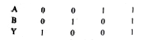
- The truth table shown in figure
Text Solution
|
- For the given combination of gates, if the logic states of inputs A,B,...
Text Solution
|
- The depletion layer in diode is 1 mum wide and the knee potential is 0...
Text Solution
|
- The current through an ideal PN junction shown in the following circui...
Text Solution
|
- The maximum effeciency of full wave rectifier is
Text Solution
|
- The emitter-base junction of a transistor is .........biased while the...
Text Solution
|
- In the case of constant alpha and beta of a transistor
Text Solution
|
- If alpha=0.98 and current through emitter i(e)=20 mA, the value of bet...
Text Solution
|
- If A and B are two inputs in AND gate, then AND gate has an output of ...
Text Solution
|
- A semiconducting device is connected in a series circuit with a batter...
Text Solution
|
- The current transfer ratio beta of a transistor is 50. The input resis...
Text Solution
|
- Value of forbidden energy gap for semi conductor is:
Text Solution
|
- GaAs is-
Text Solution
|
- Regarding a semiconductor which one of the following statements is wro...
Text Solution
|
- A strip of copper and another of germanium are cooled from room tempe...
Text Solution
|
- A light emitting diode (LED) has a voltage drop of 2V across it and pa...
Text Solution
|
- The forbidden energy band gap in conductors, semiconductors and insula...
Text Solution
|
- Which of the junction diodes shown below are forward biased ?
Text Solution
|