Text Solution
Verified by Experts


Topper's Solved these Questions
SEMICONDUCTOR DEVICES
AAKASH SERIES|Exercise EXERCISE -I (ENERGY BANDS AND CLASSIFICATION OF SOLIDS )|41 VideosSEMICONDUCTOR DEVICES
AAKASH SERIES|Exercise EXERCISE -I (P-N JUNCTION DIODE)|30 VideosSEMICONDUCTOR DEVICES
AAKASH SERIES|Exercise Problems (LEVEL-II)|9 VideosRAY OPTICS
AAKASH SERIES|Exercise PROBLEMS ( LEVEL-II)|60 VideosUNITS AND MEASUREMENT
AAKASH SERIES|Exercise PRACTICE EXERCISE|45 Videos
Similar Questions
Explore conceptually related problems
AAKASH SERIES-SEMICONDUCTOR DEVICES-EXAMPLES
- In a p-n junction, the depletion region is 400nm wide and and electric...
Text Solution
|
- Two junction diodes one of germanium (Ge) and other of sillicon (Si) a...
Text Solution
|
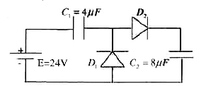
- In the circuit shown, the potential drop across each capacitor is (ass...
Text Solution
|
- A potential barrier of 0.50V exists across a p-n junction.(a) If the d...
Text Solution
|
- A potential barrier of 0.50V exists across a p-n junction.(a) If the d...
Text Solution
|
- The circuit shown in figure contains two diodes each with a forward re...
Text Solution
|
- The applied input ac power to a half wave rectifier is 100 W. The dc o...
Text Solution
|
- A p-n diode is used in a half wave rectifier with a load resistance of...
Text Solution
|
- A full wave rectifier uses two diodes with a load resistance of 100 O...
Text Solution
|
- The current through a P-N junction diode is 55mA at a forward bias vol...
Text Solution
|
- Considering the circuit and data given in the diagram calculate the cu...
Text Solution
|
- If in a p-n junction, a square input signal of 10 V is applied as show...
Text Solution
|
- For the circuit shown in Fig. find the output voltage,
Text Solution
|
- For the circuit shown in Fig. find the voltage drop across series ...
Text Solution
|
- For the circuit shown in Fig. find the current through Zener diode.
Text Solution
|
- A Zener diode is specified as having a breakdown voltage of 9.1 V,with...
Text Solution
|
- In a single state transistor amplifier, when the signal changes by 0.0...
Text Solution
|
- In a single state transistor amplifier, when the signal changes by 0.0...
Text Solution
|
- In a single state transistor amplifier, when the signal changes by 0.0...
Text Solution
|
- In a single state transistor amplifier, when the signal changes by 0.0...
Text Solution
|