Text Solution
Verified by Experts


Topper's Solved these Questions
SEMICONDUCTOR DEVICES
AAKASH SERIES|Exercise EXERCISE -I (ENERGY BANDS AND CLASSIFICATION OF SOLIDS )|41 VideosSEMICONDUCTOR DEVICES
AAKASH SERIES|Exercise EXERCISE -I (P-N JUNCTION DIODE)|30 VideosSEMICONDUCTOR DEVICES
AAKASH SERIES|Exercise Problems (LEVEL-II)|9 VideosRAY OPTICS
AAKASH SERIES|Exercise PROBLEMS ( LEVEL-II)|60 VideosUNITS AND MEASUREMENT
AAKASH SERIES|Exercise PRACTICE EXERCISE|45 Videos
Similar Questions
Explore conceptually related problems
AAKASH SERIES-SEMICONDUCTOR DEVICES-EXAMPLES
- In a transistor, the emitter circuit resistance is 100 kOmega and the...
Text Solution
|
- In the following common-emitter configuration an n-p-n transistor with...
Text Solution
|
- An n-p-n transistor in a common-emitter mode is used as a simple volta...
Text Solution
|
- The overall gain of a multistage amplifier is 100. When negative feedb...
Text Solution
|
- Calculate the gain of a negative feedback amplifier with an intern...
Text Solution
|
- Calculate the gain of a negative feedback amplifier with an intern...
Text Solution
|
- In a negative feedback amplifier ,the gain without feedback is 100,fee...
Text Solution
|
- In a negative feedback amplifier ,the gain without feedback is 100,fee...
Text Solution
|
- In a negative feedback amplifier ,the gain without feedback is 100,fee...
Text Solution
|
- In a negative feedback amplifier ,the gain without feedback is 100,fee...
Text Solution
|
- In a negative feedback amplifier ,the gain without feedback is 100,fee...
Text Solution
|
- The Boolean expression of the output y in terms of the input A and B f...
Text Solution
|
- The combination of NAND gates shown here under are equivalent to
Text Solution
|
- The diagram of a logic circuit is given below. The output of the circu...
Text Solution
|
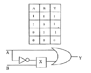
- The logic circuit and its truth table are given, what is the gate X in...
Text Solution
|
- Draw the logic circuit corresponding to the Boolean expression. Y=AB+b...
Text Solution
|
- Simplify Y = AB+ABC +barAB+ AbarBC using Boolean Algebra. Draw the res...
Text Solution
|
- Write Boolean equation for the output of fig. and solve this equation ...
Text Solution
|
- Draw logic diagrams for the Boolean expressions given below. (i)A . ...
Text Solution
|
- Draw logic diagrams for the Boolean expressions given below. (i)A . ...
Text Solution
|