Home
Class 12
PHYSICS
Transfer characteristic [output voltage ...

Transfer characteristic [output voltage `(V_(0))` vs input voltage `(V_(i))` for a base biased transistor in CE configuration is as shown in the figure. For using transistor as a switch, it is used

A

in region II

B

in region I

C

in region III

D

both in region (I) and (III)

Text Solution

Verified by Experts

The correct Answer is:
D
Promotional Banner

Topper's Solved these Questions

  • SEMICONDUCTOR DEVICES

    AAKASH SERIES|Exercise EXERCISE -I (LOGIC GATES)|17 Videos
  • SEMICONDUCTOR DEVICES

    AAKASH SERIES|Exercise EXERCISE -I (MATCHING TYPE QUESTIONS)|9 Videos
  • SEMICONDUCTOR DEVICES

    AAKASH SERIES|Exercise EXERCISE -I (P-N JUNCTION DIODE)|30 Videos
  • RAY OPTICS

    AAKASH SERIES|Exercise PROBLEMS ( LEVEL-II)|60 Videos
  • UNITS AND MEASUREMENT

    AAKASH SERIES|Exercise PRACTICE EXERCISE|45 Videos

Similar Questions

Explore conceptually related problems

Transfer characterstics [output voltage (V_(o)) vs. input voltage (V_(i)) ] for a base biased transistor in CE configuration is as shown in the figure. For using transfor as a which, it is used

Draw the tramsfer characteristic curve of a base biased transistor in CE configuration. Explain clearly how the active region of the V_o" versus " V_i curve in a transistor is used as an amplifier.

The transfer characteristics of a base biased transistor has the operation regions, namely, cutoff, active region and saturation region. For using the transistor as an amplifier it has to operate in the

What is the value of output voltage V_(0) in the circuit shown in the figure ?

The transfer characteristic curve of a transistor, having input and output resistance 100Omega and 100kOmega respectively, is shown in the figure. The Voltage and Power gain, are respectively:

The transfer characteristic curve of a transistor, having input and output resistance 100Omega and 100kOmega respectively, is shown in the figure. The Voltage and Power gain, are respectively:

Output characteristics of an n-p-n transistor in CE configuration is shown in the Fig. Determine (i) dynamic output resistance (ii) dc current gain and (iii) ac current gain at an opererating point V_(CE)=10V , when I_(B)=30muA .

In a voltage regulating of zener diode, the graph of output voltage v_(o) versus input voltage v_(1) is

Fig.shows that transfer characteristics of a base biased CE transistor. Which of the following statements are true?

Fig.shows that transfer characteristics of a base biased CE transistor. Which of the following statements are true?

AAKASH SERIES-SEMICONDUCTOR DEVICES-EXERCISE -I (TRANSISTORS)
  1. A n-p-n transistor is said to be in active region of operation, when

    Text Solution

    |

  2. Statement-I : For faster action, n-p-n transistor is used Statement-...

    Text Solution

    |

  3. A n-p-n transistor conducts when

    Text Solution

    |

  4. In a N-P-N transistor circuit, the collector current is 10 mA.If 90 % ...

    Text Solution

    |

  5. In the circuit symbol of transistor the arrow on the emitter indicates

    Text Solution

    |

  6. When a n-p-n transistor is used as an amplifier, then

    Text Solution

    |

  7. When a n-p-n transistor is used as an amplifier, then

    Text Solution

    |

  8. Which of the following statement is true for a p-n-p transistor when u...

    Text Solution

    |

  9. In CE configuration transistor, the current gain

    Text Solution

    |

  10. The transistor parameters, namely alpha and beta of a transistor are ...

    Text Solution

    |

  11. In which of the configuration of a transistor , the power gain is high...

    Text Solution

    |

  12. Transistor input characteristics curves are the graphs drawn with

    Text Solution

    |

  13. Transistor output characteristic curves are the graphs drawn with

    Text Solution

    |

  14. The circuit diagram below shows n-p-n transistor in CE configuration. ...

    Text Solution

    |

  15. Consider a p-n junction as a capacitor, formed with p and n - material...

    Text Solution

    |

  16. In a common base amplifier the phase difference the input signal volta...

    Text Solution

    |

  17. For a transistor amplifier, the voltage gain

    Text Solution

    |

  18. An electrical device draws 0.968 kW form AC mains of 220 V.If current ...

    Text Solution

    |

  19. To use a transistor as an amplifier

    Text Solution

    |

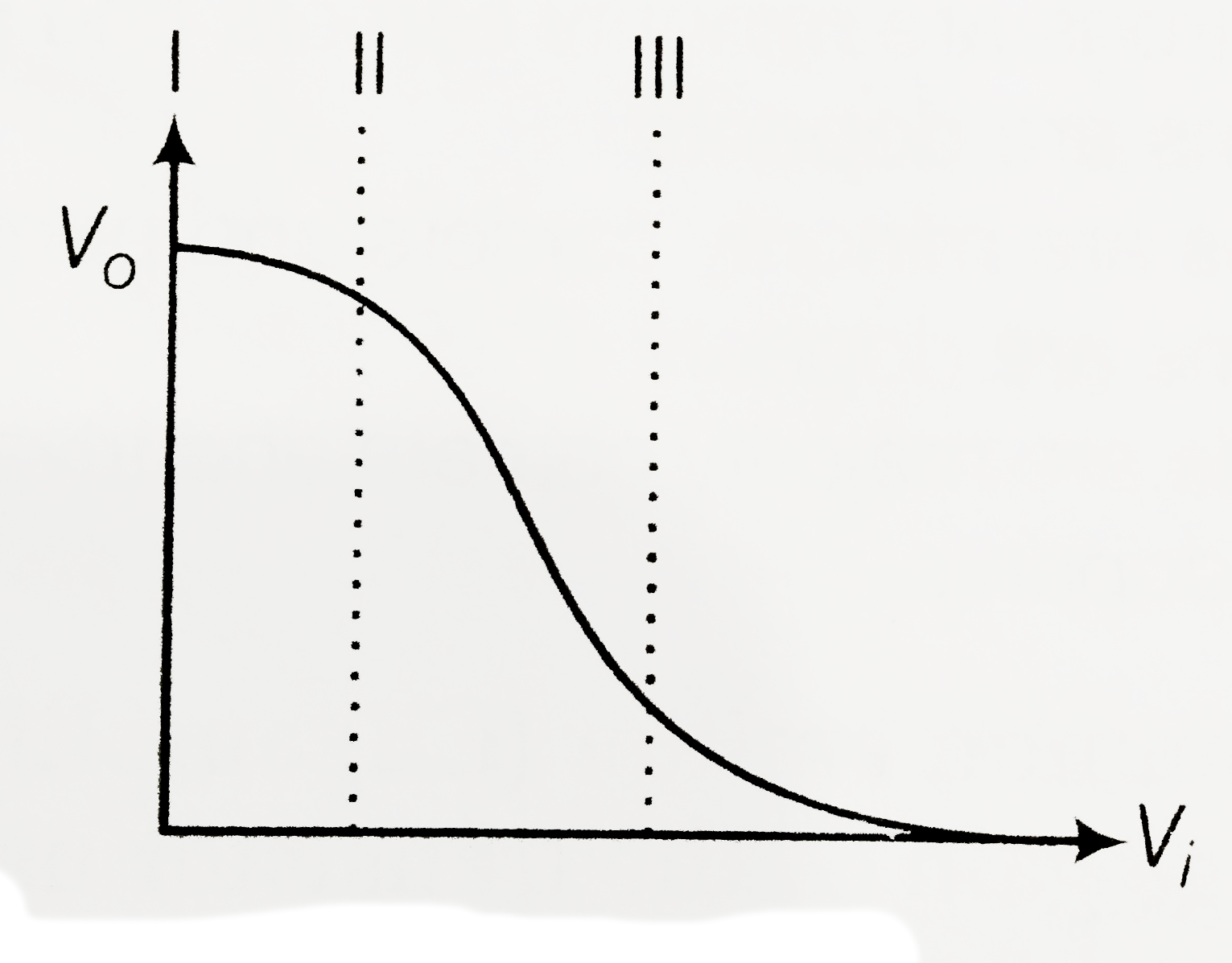
  20. Transfer characteristic [output voltage (V(0)) vs input voltage (V(i))...

    Text Solution

    |