A
B
C
D
Text Solution
Verified by Experts
The correct Answer is:


Topper's Solved these Questions
SEMICONDUCTOR ELECTRONICS: MATERIALS, DEVICES AND SIMPLE CIRCUITS
AAKASH INSTITUTE|Exercise Assignment (Section -B (Objective type question (one option is correct))|29 VideosSEMICONDUCTOR ELECTRONICS: MATERIALS, DEVICES AND SIMPLE CIRCUITS
AAKASH INSTITUTE|Exercise Assignment (Section -C(Linked comprehension type question))|3 VideosSEMICONDUCTOR ELECTRONICS: MATERIALS, DEVICES AND SIMPLE CIRCUITS
AAKASH INSTITUTE|Exercise Try yourself|20 VideosSEMICONDUCTOR ELECTRONICS (MATERIAL, DEVICES AND SIMPLE CIRUITS )
AAKASH INSTITUTE|Exercise Assignment SECTION - D (Assertion & reason type Question)|10 VideosSYSTEM OF PARTICLES AND ROTATIONAL MOTION
AAKASH INSTITUTE|Exercise Try Yourself|63 Videos
Similar Questions
Explore conceptually related problems
AAKASH INSTITUTE-SEMICONDUCTOR ELECTRONICS: MATERIALS, DEVICES AND SIMPLE CIRCUITS-Assignment (Section -A (Objective Type question (One option is correct))
- Serious draw back of the semiconductor device is
Text Solution
|
- The reason of current flow in P-N junction forward biase is
Text Solution
|
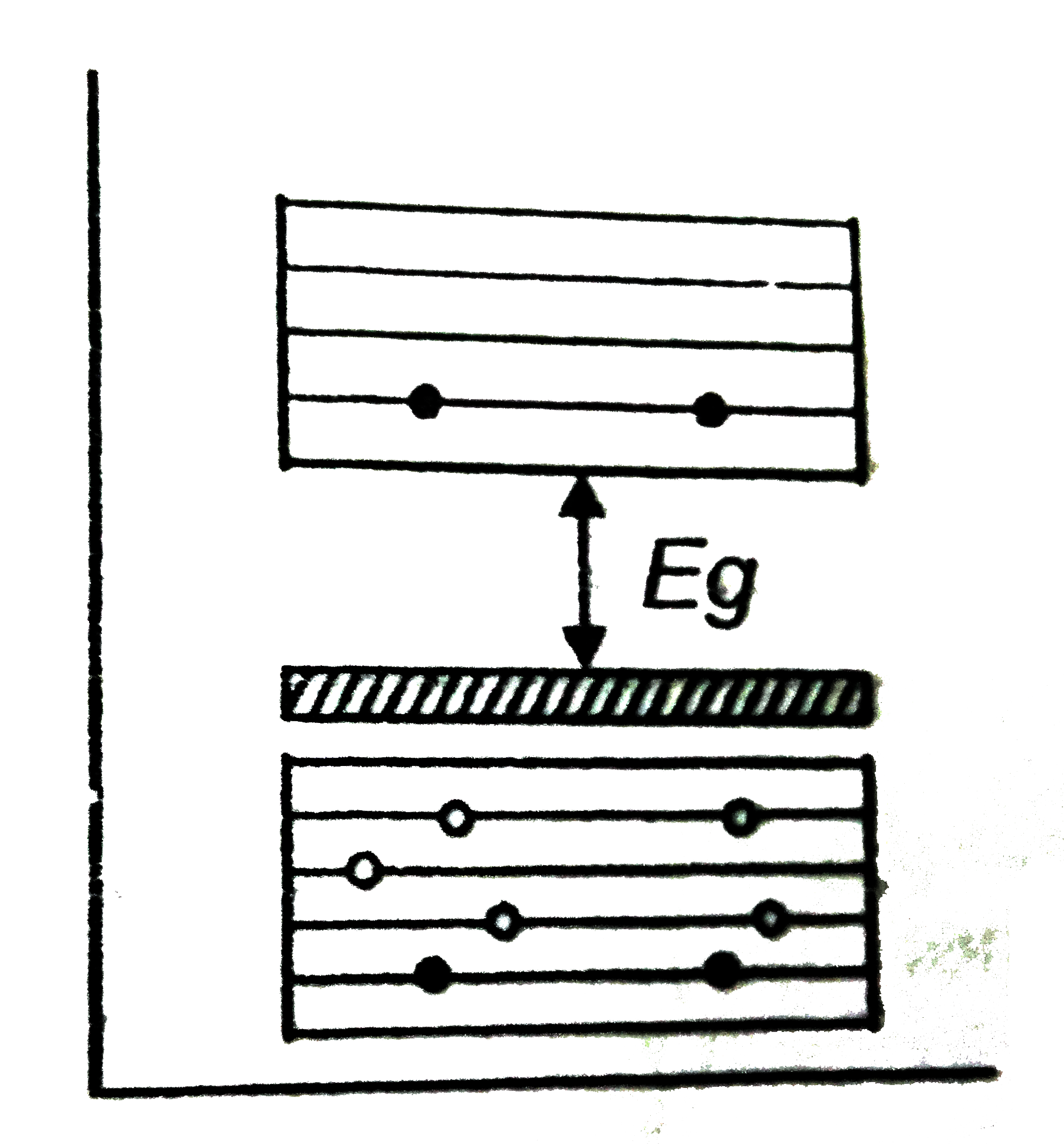
- In the energy band diagram of a material shown below, the open circles...
Text Solution
|
- An oscillator is nothing but an amplifier with
Text Solution
|
- When n-p-n transistor is used as an amplifier
Text Solution
|
- If l(1),l(2),l(3) are the lengths of the emitter, base and collector o...
Text Solution
|
- a common emitter amplifier gives an output of 3V for an input of 0.01 ...
Text Solution
|
- In a common emitter amplifier, the phase difference between the input ...
Text Solution
|
- In a common emitter amplifier the input signal is applied across
Text Solution
|
- The concentration of impurities in a transistor is
Text Solution
|
- In a transistor, the collector current is always · less then the emitt...
Text Solution
|
- The minimum potential difference between the base and emitter required...
Text Solution
|
- Which of the following represents NAND gate ?
Text Solution
|
- The circuit is equivalent to
Text Solution
|
- The output y, when all three inputs are first high and then low, will ...
Text Solution
|
- A silicon specimen is made into a P-type semiconductor by doping, on a...
Text Solution
|
- Consider the junction diode is ideal. The value of current through the...
Text Solution
|
- Negative feedback
Text Solution
|
- The current obtained from a simple filterless reactifier is
Text Solution
|
- The depletion region of p-n junction has a thickness of the order of
Text Solution
|