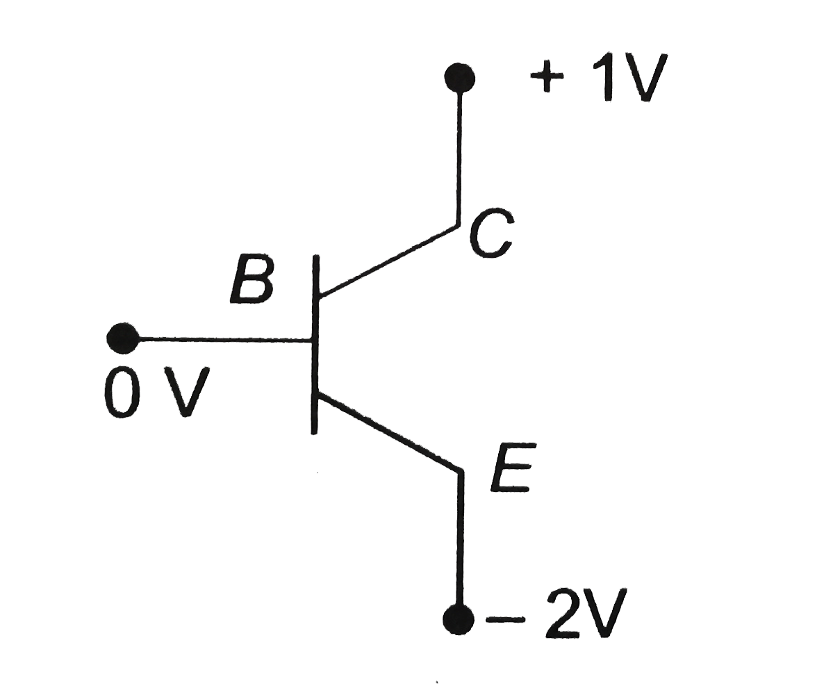
A
B
C
D
Text Solution
Verified by Experts
The correct Answer is:


Topper's Solved these Questions
SEMICONDUCTOR ELECTRONICS
A2Z|Exercise AIPMT/NEET Questions|77 VideosSEMICONDUCTOR ELECTRONICS
A2Z|Exercise AIIMS Questions|38 VideosSEMICONDUCTOR ELECTRONICS
A2Z|Exercise Problems Based On Mixed Concepts|32 VideosNUCLEAR PHYSICS
A2Z|Exercise Section D - Chapter End Test|29 VideosSOURCE AND EFFECT OF MAGNETIC FIELD
A2Z|Exercise Section D - Chapter End Test|30 Videos
Similar Questions
Explore conceptually related problems
A2Z-SEMICONDUCTOR ELECTRONICS-Section B - Assertion Reasoning
- Assertion : An N-type semiconductor has a large number of electrons bu...
Text Solution
|
- Assertion : The crystalline solids have a sharp melting point. Reaso...
Text Solution
|
- Assertion: Silicon is preferred over germanium for making semiconducto...
Text Solution
|
- Assertion: Two P-N junction diodes placed back to back, will work as a...
Text Solution
|
- Assertion : In transistor common emitter mode as an amplifier is pref...
Text Solution
|
- Assertion:The dominant mechanism for motion of charge carriers in forw...
Text Solution
|
- Assertion: A transistor is a voltage-operating device. Reason: Base ...
Text Solution
|
- Assertion: NAND or NOR gates are called digital building blocks. Rea...
Text Solution
|
- Assertion: At 0K germanium is a superconductor. Reason: At 0K german...
Text Solution
|
- Assertion: Base in transistor is made very thin as compared to collect...
Text Solution
|
- Assertion: The current gain in common base circuit is always less than...
Text Solution
|
- Assertion: V-i charcteristic of P-N junction diode is same as that of ...
Text Solution
|
- Assertion: Zener diode works on a principle of of breakdown voltage. ...
Text Solution
|
- Assertion: NOT gate is also called inverter circuit. Reason: NOT gat...
Text Solution
|
- Assertion: In vacuum tubes (vales), vacuum is necessary for the moveme...
Text Solution
|
- Assertion: The following circuit represents 'OR' gate Reason: For...
Text Solution
|
- Assertion: A P-N photodiode is made from a semiconductor for which E(...
Text Solution
|
- Assertion: When PN-junction is forward biased then motion of charge ca...
Text Solution
|
- Assertion: De Morgan's theoram bar(A+B)=bar(A).bar(B) may be explained...
Text Solution
|
- Assertion: In the following circuit the potential drop across the resi...
Text Solution
|