Text Solution
Verified by Experts


Topper's Solved these Questions
SEMICONDUCTOR ELECTRONICS METERIALS DEVICES AND SIMPLE CIRCUITS
MODERN PUBLICATION|Exercise TOUGH & TRICKY PROBLEMS|10 VideosSEMICONDUCTOR ELECTRONICS METERIALS DEVICES AND SIMPLE CIRCUITS
MODERN PUBLICATION|Exercise NCERT FILE SOLVED (TEXT BOOK EXERCISES )|30 VideosSEMICONDUCTOR ELECTRONICS METERIALS DEVICES AND SIMPLE CIRCUITS
MODERN PUBLICATION|Exercise PRACTICE PROBLEMS|26 VideosRAY OPTICS AND OPTICAL INSTRUMENTS
MODERN PUBLICATION|Exercise CHAPTER PRACTICE TEST|14 VideosWAVE OPTICAL
MODERN PUBLICATION|Exercise CHAPTER PRACTICE TEST|7 Videos
Similar Questions
Explore conceptually related problems
MODERN PUBLICATION-SEMICONDUCTOR ELECTRONICS METERIALS DEVICES AND SIMPLE CIRCUITS -CONCEPUAL QUESTIONS
- A p n junction diode is connected to a battery of 2 v and a resistanc...
Text Solution
|
- A p -n junctin diode is connected to a battery of 2 V and a resistan...
Text Solution
|
- A half wave rectifier provides DC output power of 30 W when 100 W AC ...
Text Solution
|
- How can we use a diode as a switch
Text Solution
|
- How can we increase the intensity of an LED
Text Solution
|
- In a transistor base is made thin and doped with little impurity atoms...
Text Solution
|
- How will the current in the transistor change with the increase in...
Text Solution
|
- Explain, why the input resistance of a transistor is low and output re...
Text Solution
|
- Transistor also works bidirectinaly commment
Text Solution
|
- In a transistor both emitter base jucntion and colector base junction ...
Text Solution
|
- If the base region of a transistor is made large, as compared to a usu...
Text Solution
|
- In the given circuit diagram, a voltmeter 'V' is connected across a la...
Text Solution
|
- How are analogue and digital signals different
Text Solution
|
- Discuss how a NOT gate is realised using NAND gates.
Text Solution
|
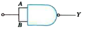
- Realise the formation of AND gate using NAND gate
Text Solution
|
- Realise the formation of OR gate from NAND gate
Text Solution
|
Text Solution
|
- NAND gate is also known as digital building block explain
Text Solution
|
- Arrange two NAND gates and one OR gate such that the combination o...
Text Solution
|
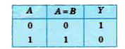
- The following Fig. shows the input waveforms (A,B) and the output wave...
Text Solution
|