Home
Class 12
PHYSICS
Using the necessary circuit diagram, sho...

Using the necessary circuit diagram, show how the V-I characteristics of a p-n junction are obtained in (i) forward biasing (ii) Reverse biasing. How are these characteristics made use of in rectification?

Text Solution

Verified by Experts

(a) (i) p-n junction diode under forward bias:
The V-I characteristics of p-n junction in forward bias is shown below:
p-side is connected to the positive terminal and n-side to the negative terminal.
Applied voltage drops across the depletion region.
Electron in n-region moves towards the p-n junction and holes in the p-region move towards the junction. The width of the depletion layer decreases and hence, it offers less resistance.
Diffusion of majority carriers takes place across the junction. This leads to the forward current.


(ii) p-n junction under reverse bias :
Positive terminal of battery is connected to n-side and negative terminal to p-side
Reverse bias supports the potential barrier. Therefore, the barrier height increases and the width of depletion region also increases.
Due to the majority carriers, there is no conduction across the junction. A few minority carriers cross the junction after being accelerated by high reverse bias voltage.

This constitutes a current flows in opposite direction, which is called reverse current.
The V-I characteristics of p-n junction diode in reverse bias is shown on previous page.
p-n junction diode is used as a half-wave rectifier. Its working is based on the fact that the resistance of p-n junction becomes low when forward biased an becomes high when reverse biased. These characteristics of diode is used in rectification.
Promotional Banner

Topper's Solved these Questions

  • XII BOARDS

    XII BOARDS PREVIOUS YEAR|Exercise [SET - II DELHI BOARD]|6 Videos
  • XII BOARDS

    XII BOARDS PREVIOUS YEAR|Exercise [SET - III, DELHI BOARD]|6 Videos
  • XII BOARDS

    XII BOARDS PREVIOUS YEAR|Exercise SET - III (Delhi Board)|8 Videos
  • SAMPLE PAPER 2019

    XII BOARDS PREVIOUS YEAR|Exercise SECTION D|6 Videos

Similar Questions

Explore conceptually related problems

(a) state briefly the processes involved in the formation of p-n how the depletion region is formed (b) using the necessary ciruit diagrams show p-n jucntion are obtained in (i) forward biasing (ii) reverse biasing how these characteiistics are made use of in recitifcation

In V - I characteristics of p-n junction in reverse biasing results in

(a). Explains briefly with the help of a circuit diagram how V-I characteristics of a p-n junction diode are obtainedin (i) forward bias, and (ii) reverse bias. (b). A photo diode is fabricated from a semiconductor with a band gap of 2.8 EV. Can it detect wave length of 6000. nm? Justify.

P-N junction biasing and characteristics

What happens to the width of depletion layer of a p-n junction when it is (i) forward biased, (ii) reverse biased?

What is the deffect on current when a p-n diode is (i) forward biased (ii) reverse biased

XII BOARDS PREVIOUS YEAR-XII BOARDS-[SET - I]
  1. Identify the logic gates marked P and Q in the circuit Fig. Write the ...

    Text Solution

    |

  2. A capacitor C, a variable resistor R and a bulb B are connected in ser...

    Text Solution

    |

  3. A proton and deutron are accelerated through the same accelerating pot...

    Text Solution

    |

  4. (i) Mono chromatic light of frequency 6.0xx10^(14)Hz is produced by a ...

    Text Solution

    |

  5. A 12/5 eV electron beam is used to bombard gaseous hydrogen at room te...

    Text Solution

    |

  6. When Sunita, a class XII student, came to know that her parents are pl...

    Text Solution

    |

  7. A potentiometer wire of length 1 m has a resistance of 10Omega. It is ...

    Text Solution

    |

  8. (a) Draw a labelled ray diagram showing the formation of a final image...

    Text Solution

    |

  9. (a) A mobile phone lies along the principal axis of a concave mirror. ...

    Text Solution

    |

  10. (a) How is a toroid different from a solenoid? (b) Show that in an i...

    Text Solution

    |

  11. Derive an expression for the magnetic moment (vec mu) of an electron r...

    Text Solution

    |

  12. (a) State Ampere's circuital law, expressing it in the integral form. ...

    Text Solution

    |

  13. Answer the following : (a) Name the em waves which are suitable for ...

    Text Solution

    |

  14. Deduce the expression, N=N(0)^(-lambdat) for the law of radioactive de...

    Text Solution

    |

  15. (a) (i) Two independent mono chromatic sources of light cannot produc...

    Text Solution

    |

  16. (a) How does one demonstrate, using a suitable diagram, that unpolaris...

    Text Solution

    |

  17. (a) Describe a simple experiment (or activity) to show that the polari...

    Text Solution

    |

  18. Draw a schematic sketch of an generator describing its basic elements....

    Text Solution

    |

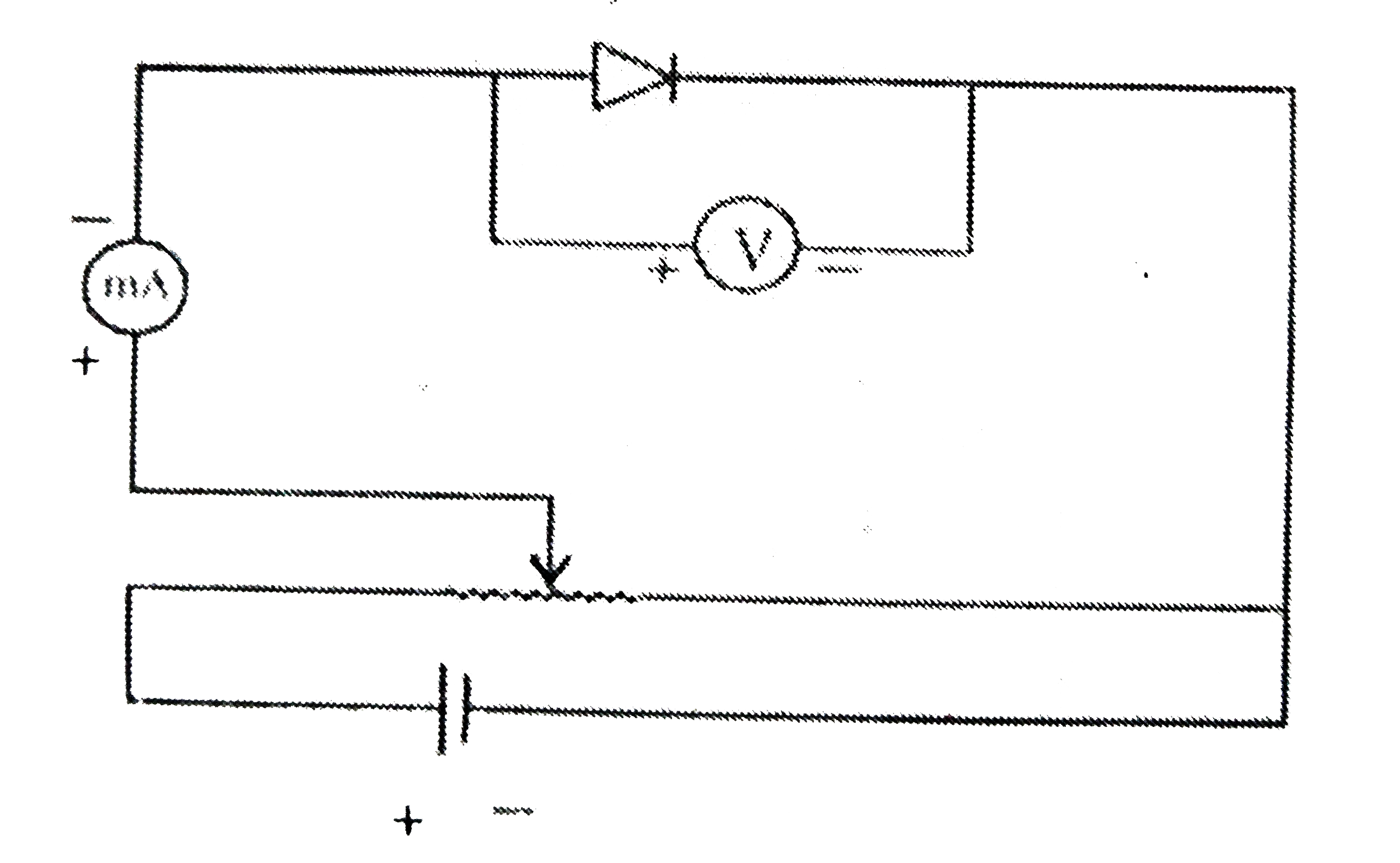
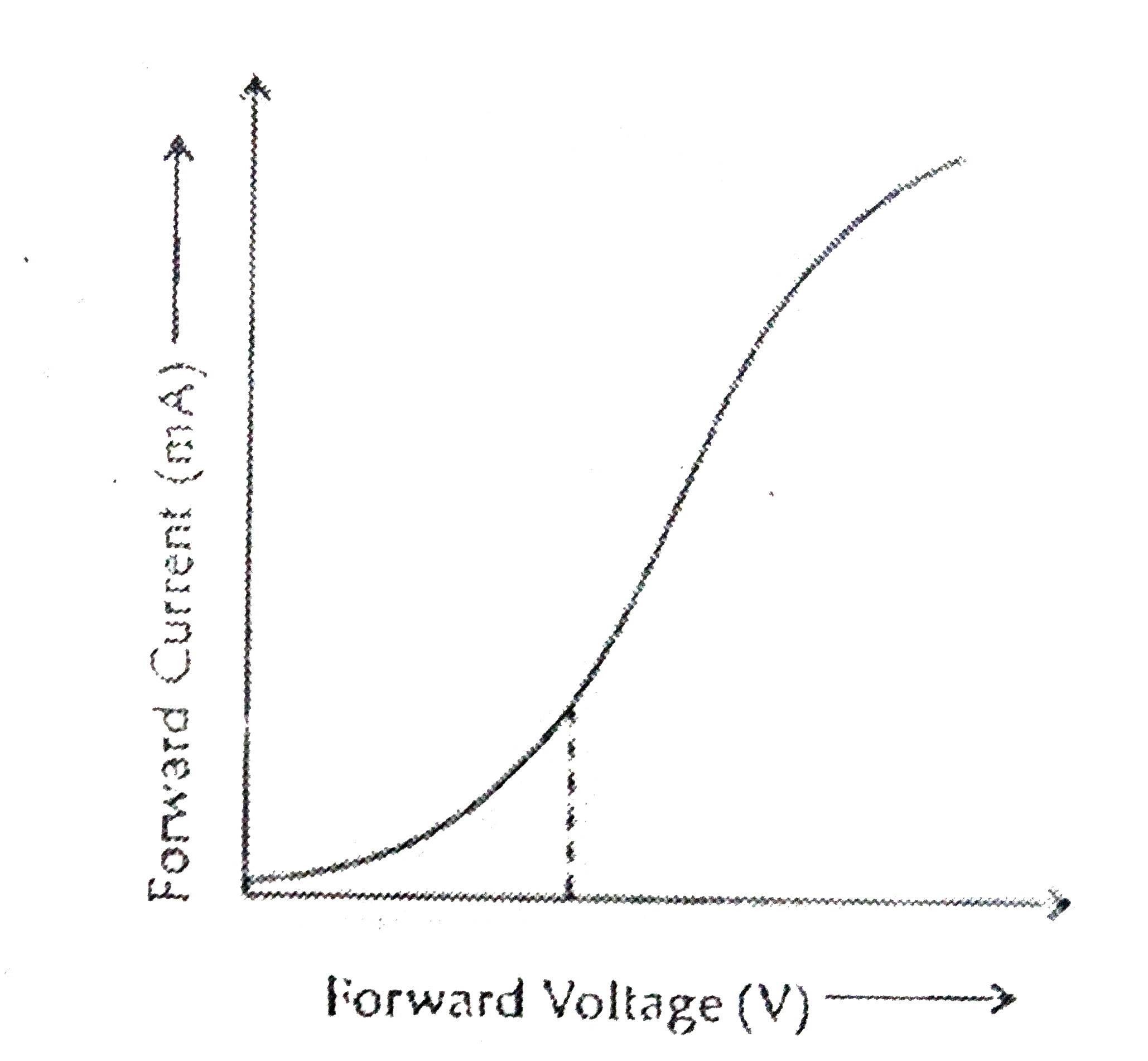
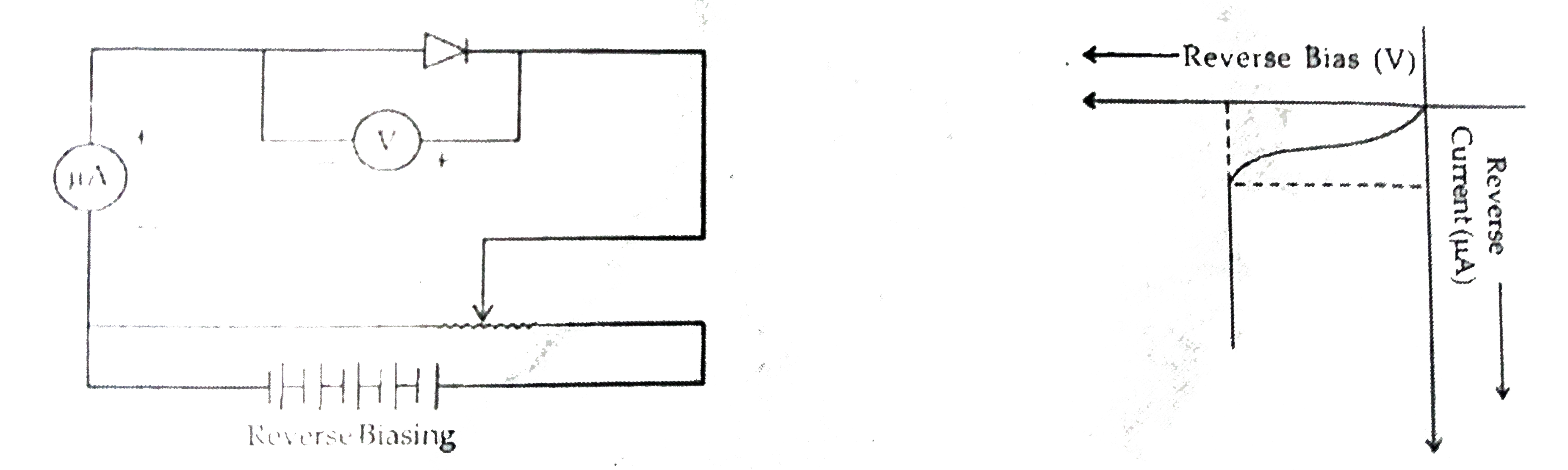
  19. Using the necessary circuit diagram, show how the V-I characteristics ...

    Text Solution

    |

  20. (a) Differentiate between three segments of a transistor on the basis ...

    Text Solution

    |