A
B
C
D
Text Solution
Verified by Experts
The correct Answer is:


Topper's Solved these Questions
SOLIDS & SEMICONDUCTOR DEVICES
MODERN PUBLICATION|Exercise Multiple Choice Questions - LEVEL -I (ASSERTION)|5 VideosSOLIDS & SEMICONDUCTOR DEVICES
MODERN PUBLICATION|Exercise Multiple Choice Questions - LEVEL -I (PARAGRAPH)|6 VideosROTATIONAL MOTION
MODERN PUBLICATION|Exercise RCQ|8 VideosTRANSFERENCE OF HEAT
MODERN PUBLICATION|Exercise Recent Competitive Questions|4 Videos
Similar Questions
Explore conceptually related problems
MODERN PUBLICATION-SOLIDS & SEMICONDUCTOR DEVICES-Revision Test
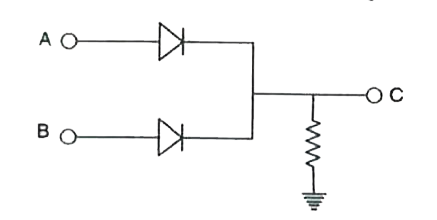
- In the circuit below , A and B represent two inputs and C represents t...
Text Solution
|
- Choose the forward biased p-n junction :
Text Solution
|
- Choose the reverse biased p-n junction :
Text Solution
|
- The forward biased characteristics of a p - n junction are :
Text Solution
|
- If Ie is emitter current , Ib is base current and Ic is the collector ...
Text Solution
|
- Zener diode is :
Text Solution
|
- The reverse biased characteristics of a p-n junction are :
Text Solution
|
- The advantage of BJT (Bipolar junction transistor) over vacuum tube tr...
Text Solution
|
- For an unknown element , the thickness of forbidden band is 4.97 eV an...
Text Solution
|
- At abosolute zero, a metal will behave as :
Text Solution
|
- A piece aluminium and germanium each, are cooled from T1 K to T2 K . T...
Text Solution
|
- One speaks of mutual characteristics in connection with L :
Text Solution
|
- In a frequency modulated wave :
Text Solution
|
- A small portion of Indium is incorporated is germanium . The crystal w...
Text Solution
|
- In a transistor the base is made very thin and a very hightly doped ...
Text Solution
|
- The safety limit of temperature for germanium and silicon are :
Text Solution
|
- A semiconductor diode designed to operate in breakdown region is calle...
Text Solution
|
- Power consumed by an ideal diode is :
Text Solution
|
- A conductor at very high temperature becomes :
Text Solution
|
- Zenor breakdown semiconductor
Text Solution
|
- Conduction - electron have more mobility than holes because these elec...
Text Solution
|