A
B
C
D
Text Solution
Verified by Experts
The correct Answer is:


Topper's Solved these Questions
SOLIDS & SEMICONDUCTOR DEVICES
MODERN PUBLICATION|Exercise Multiple Choice Questions - LEVEL -III (Questions From AIEEE/JEE Examination)|9 VideosSOLIDS & SEMICONDUCTOR DEVICES
MODERN PUBLICATION|Exercise Recent Competitive Questions|26 VideosSOLIDS & SEMICONDUCTOR DEVICES
MODERN PUBLICATION|Exercise Multiple Choice Questions - LEVEL -I (PARAGRAPH)|6 VideosROTATIONAL MOTION
MODERN PUBLICATION|Exercise RCQ|8 VideosTRANSFERENCE OF HEAT
MODERN PUBLICATION|Exercise Recent Competitive Questions|4 Videos
Similar Questions
Explore conceptually related problems
MODERN PUBLICATION-SOLIDS & SEMICONDUCTOR DEVICES-Multiple Choice Questions - LEVEL -II
- The contribution in the total current flowing through a semiconductor ...
Text Solution
|
- Ge and Si diode conduct at 0.3 V and 0.7respectively . In the followi...
Text Solution
|
- In the circuit shown in figure the maximum output voltage
Text Solution
|
- In the following circuit find I1 and I2
Text Solution
|
- The following configuration of gate is equivalent to :
Text Solution
|
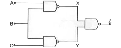
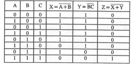
- Figure gives a system of logic gates . From the study of truth table i...
Text Solution
|
- The combination of gates shown below produces
Text Solution
|
- The figure shows NAND gates followed by a NOR gate . The system is equ...
Text Solution
|
- The diagram of a logic circuit is given below . The output F of the ci...
Text Solution
|
- The voltage gain of the following amplifier is
Text Solution
|
- An alternating voltage of 141.4 V (rms) is applied to a vacuum diode a...
Text Solution
|
- The plate current in a triode is given be Ip=0.004 (Vp+10Vg)^(3//2)mA ...
Text Solution
|
- For an amplifier in C.E. configuration for load 1kOmega (h(fe)=50) and...
Text Solution
|
- In a full wave rectifier with input frequency 50 Hz the ripple in the ...
Text Solution
|
- The electrical conductivity of a semiconductor increases when electrom...
Text Solution
|
- If ratio of concentration of electrons to that of holes in a semicondu...
Text Solution
|
- In a common base mode of a transistor, the collector current is 5.488 ...
Text Solution
|
- A p - n junction (D) shown in the figure can act as a rectifier . An a...
Text Solution
|
- The logic circuit shown below has the input waveform 'A' and 'B' as sh...
Text Solution
|
- The combination of gates shown below yields :
Text Solution
|